
High Frequency PCB Manufacturing
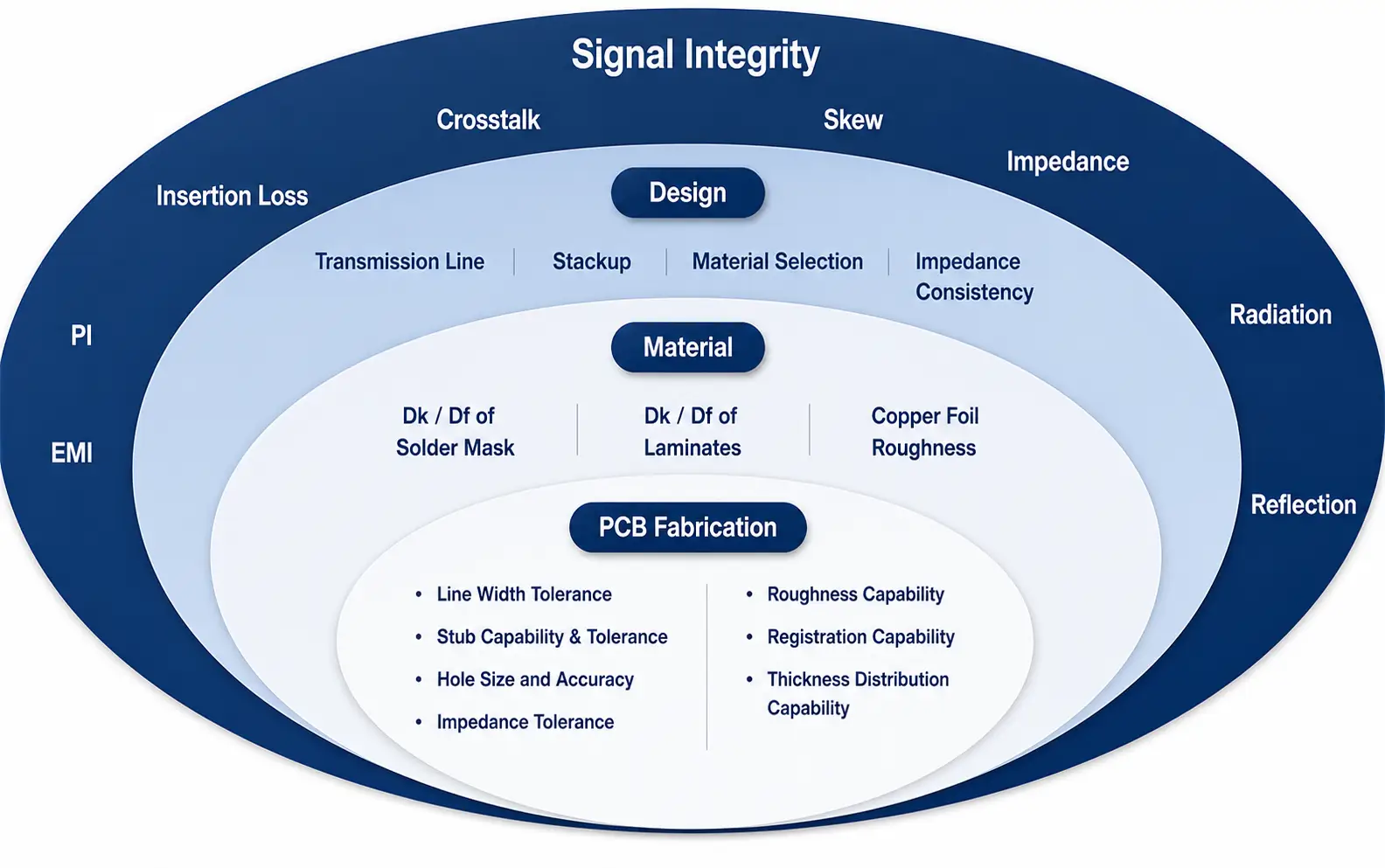
Signal integrity is the foundation of high frequency PCB performance.
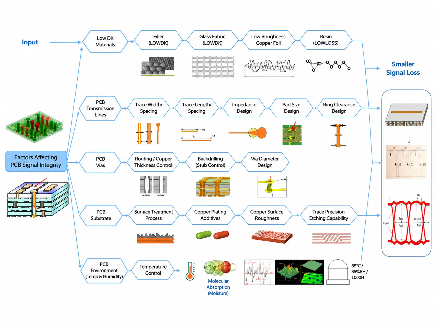
ShinePCB manufactures high frequency PCBs using low-Dk and low-Df materials, advanced impedance control techniques, ultra-low roughness copper foil, and optimized PCB stack-up structures. These processes help reduce insertion loss, minimize signal reflection, and improve overall transmission efficiency.
We specialize in multilayer RF boards, microwave circuits, high-speed backplanes, 5G infrastructure, optical networking equipment, and AI server applications requiring superior electrical performance.
High Frequency PCB
High frequency PCBs are designed for RF, microwave, millimeter-wave, and high-speed digital applications where signal integrity and low transmission loss are critical. These boards are widely used in 5G infrastructure, automotive radar, satellite communications, data centers, and aerospace systems.
Materials
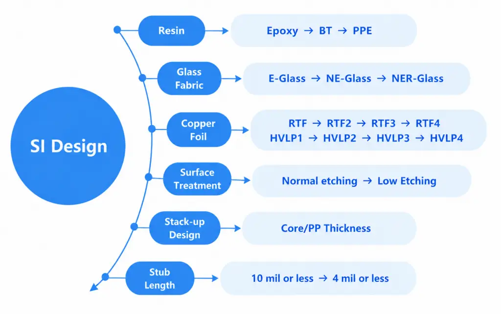
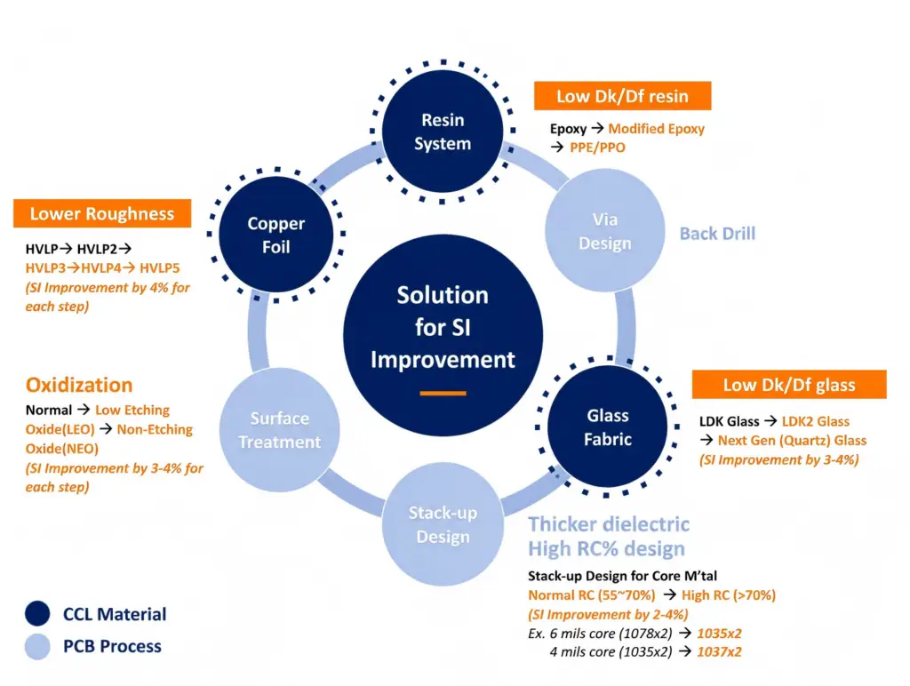
ShinePCB supports a wide range of low-loss materials, including Rogers, Taconic, Isola, Panasonic Megtron, and PTFE laminates. Material selection is optimized according to frequency range, dielectric requirements, and application-specific performance targets.
Advantages
• Controlled Impedance Manufacturing
• Low-Loss Material Expertise
• Ultra-Low Profile Copper Foil
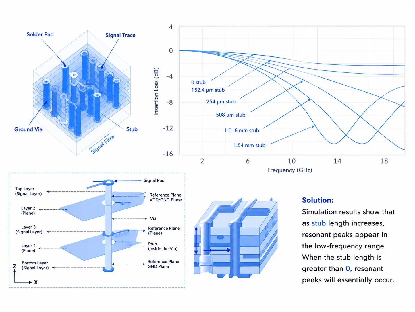
• Back Drilling & Signal Integrity Optimization
• Hybrid Stack-Up Capability
• RF and Microwave PCB Experience
• Rapid Prototype to Volume Production
ShinePCB bridges the gap between signal integrity design and manufacturing execution.
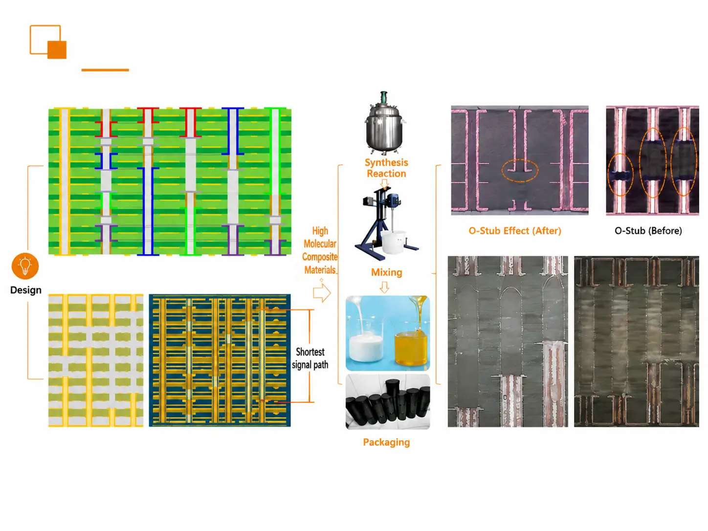
Our engineering team works directly with customers to optimize material selection, stack-up architecture, impedance structures, copper foil roughness, dielectric systems, and back-drilling strategies before production begins. Every design recommendation is evaluated against actual manufacturing capabilities to ensure predictable and repeatable electrical performance.
By integrating SI simulation knowledge with full-process PCB fabrication expertise, we help customers reduce insertion loss, minimize signal reflection, improve impedance consistency, and accelerate design validation for high-speed and high-frequency applications.
High Frequency PCB Expertise Engineered for Superior Signal Integrity
ShinePCB specializes in high frequency PCB manufacturing for RF, microwave, high-speed digital, and 5G communication applications. By combining low-loss materials, controlled impedance technologies, advanced stack-up design, and precision fabrication processes, we deliver reliable electrical performance for demanding environments.
10GHz+
RF & Microwave Applications
Low Loss
Optimized Signal Transmission
HDI & RF
Advanced PCB Structures
Advanced High Frequency PCB Manufacturing
ShinePCB provides comprehensive high frequency PCB manufacturing solutions covering material selection, stack-up design, impedance control, copper roughness optimization, back drilling, stub reduction, and advanced fabrication processes.
From low-loss laminates and RF structures to precision routing and multilayer signal integrity optimization, our engineering team supports every stage of production to minimize insertion loss, reduce reflection, and ensure reliable high-speed performance.
With complete in-house manufacturing capabilities, we deliver prototype and volume production for RF, microwave, 5G, AI server, optical networking, aerospace, and automotive radar applications.
Low Dk/Df
Rogers • Taconic • PTFE • Megtron
Full Process
Materials • Design • Fabrication
One-Stop
From Material Selection to Mass Production
Our 5-D Process
01.
Submit Your Inquiry
Click the “Get a Quote” button on our home page, upload your Gerber file, and input the full details of your specification requirements.
02.
Engineering Audit
Your inquiry will be sent directly to our internal system for an engineering review. Our team will evaluate the files and contact you to ensure all technical specifications are met.
03.
Quote Confirmation
Once the audit is complete, we will send the formal quotation and payment instructions via email. You can confirm with us directly by replying to the email. (For payment inquiries, please contact: info@.com)
04.
Track Your Progress
After the order is placed, you can track its production progress online at any time. Our engineers will perform a final review before production and notify you of any discrepancies.
05.
Deliver
Once your order is confirmed, you can monitor its real-time status through our online system. Before fabrication begins, our engineering team conducts a specialized final review and will promptly contact you regarding any technical discrepancies. Every shipment is backed by a secondary centralized 100% inspection to guarantee that your high-precision boards meet all specifications before they leave our facility.
Product terminals
Leveraging our extensive industry expertise, we consistently deliver to the highest rigorous standards. Our footprint spans a diverse range of market segments, including Telecom, Datacom, Computer & Storage, Medical, Mil/Aero, Industrial, and Consumer Electronics.
Supported Certifications
Satellite Communication
Telecom Infrastructure
Consumer Electronics
UAV Systems
Power & Energy
Medical Electronics
Networking Equipment
Reliable PCB Quality Control and Inspection
Shine PCB implements strict PCB quality control procedures, including AOI inspection, X-ray analysis, impedance testing, and final electrical verification to ensure stable performance and long-term reliability.