
PCB Solutions Provider
High-Performance PCB, Turnkey Assembly & BOM Services
Advanced PCB Materials
Manufacturing high-frequency, RF, HDI, and high-speed PCBs using Rogers, Isola, Shengyi, and other premium laminates. Suitable for telecommunications, industrial control, automotive, and aerospace applications.
Turnkey PCB Assembly
Complete PCB assembly services including PCB fabrication, BOM sourcing, SMT, THT, testing, and final delivery. One supplier, one workflow, faster production.
Engineering Support
DFM review, BOM optimization, alternative component sourcing, and manufacturing consultation to reduce risk and improve product reliability.
Quality & Compliance
ISO-certified manufacturing with AOI inspection, electrical testing, RoHS compliance, and full production traceability for every order.
Power Your Vision with China Precision
Quality Services
High-Frequency & High-Speed
Rogers / TUC / Isola
Plasma Desmear Process
Low-Dk / Low-Df Materials
Asymmetric / Hybrid Lamination
Ultra-Large Size
1000mm x 600mm Ultra-Large Size
Contour Precision Tolerance: ±0.05mm
Pattern Alignment Accuracy: ±3mil
Solder Mask Registration: ±2mil
Warpage: ≤0.5%
Heavy Copper
Heavy Copper & Selective Thick Copper Process
Maximum 15oz Heavy Copper Thickness
High Heat Dissipation & Low Thermal Strain
Microcrystalline Phosphor Copper Spheres
HDI
Laser Drilling & VCP Filling
Minimum Trace Width/Spacing: 2/2mil
Special Features: Back-Drilling & Cavity Boards
PCB Fabrication & Turnkey PCB Assembly
We Follow Best Practices
China’s Leading Turnkey Solution for Global Innovation
- Elite Ecosystem
- Rapid Turnaround
- Advanced SMT/PCB
- Zero-Defect Goal
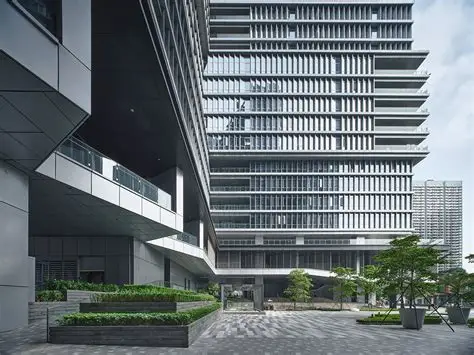
About Shine PCB
With 20 years of industry expertise, Shine PCB stands at the heart of China, the world’s premier hub for printed circuit board production. By integrating the region’s elite manufacturing capabilities, we provide comprehensive EMS and OEM solutions tailored for global innovation. Specializing in high-efficiency turnkey solutions for small to medium volumes.
We excel in high-complexity manufacturing, including 4 to 48-layer boards, HDI with blind/buried vias, and high-frequency substrates. Leveraging South China’s leading material supply chain, we ensure superior thermal stability and signal integrity in every build. Our facilities are fully certified by ISO 9001, ISO 13485, UL, and RoHS, meeting the most exacting industry standards.
Our Supply Chain Partners
Partnering with Leading Global Material and Component Suppliers
Business Partners
Supporting Innovation Across Global Electronics Industries
We Offer Comprehensive BOM and Component Sourcing Services
One-Stop Electronics Supply Chain
Supported Certifications
Certification certificates can be provided upon request. Please contact our sales or support team for further information.


Product terminals
Leveraging our extensive industry expertise, we consistently deliver to the highest rigorous standards. Our footprint spans a diverse range of market segments, including Telecom, Datacom, Computer & Storage, Medical, Mil/Aero, Industrial, and Consumer Electronics.
Supported Certifications
Satellite Communication
Telecom Infrastructure
Consumer Electronics
UAV Systems
Power & Energy
Medical Electronics
Networking Equipment
Request a Quote
How to order the PCBs on ShinE?
How to Order
We encourage customers to initiate their projects via our online inquiry system. You can complete the process in four simple steps.
Step 1: Submit Your Inquiry Click the “Get a Quote” button on our home page, upload your Gerber file, and input the full details of your specification requirements.
Step 2: Engineering Audit Your inquiry will be sent directly to our internal system for an engineering review. Our team will evaluate the files and contact you to ensure all technical specifications are met.
Step 3: Quote Confirmation & Payment Once the audit is complete, we will send the formal quotation and payment instructions via email. You can complete the payment in the “Awaiting Payment” zone or confirm with us directly by replying to the email. (For payment inquiries, please contact: info@pcbonline.com)
Step 4: Track Your Progress After the order is placed, you can track its production progress online at any time. Our engineers will perform a final review before production and notify you of any discrepancies.
Can I modify the order quantity?
Before payment, you can inform our online customer service on the right of every page to change the quantity and price.
For the placed order, we will arrange the production for the first time, so the quantity cannot be modified, but if you want to add quantity, you can place another order. We will try to arrange delivery to you together.
What do I need to offer you when I place an order on ShinePCB?
To avoid any unnecessary delays, please ensure the following information is provided before submitting your order:
PCB Material
Please specify the material to be used, including but not limited to FR-4, aluminum, FPC, or rigid-flex PCB.PCB Layer Count
Please confirm the number of layers required, such as single-sided, double-sided, 4-layer, 6-layer, or 8-layer PCB.Board Thickness
Please specify the board thickness, for example: 0.8mm, 1.0mm, 1.2mm, 1.6mm, or 2.0mm.Copper Thickness
Please confirm the copper weight/thickness required, such as 1oz, 2oz, or 3oz.Surface Finish
Please specify the preferred surface finish, including HASL Lead-Free, ENIG (Immersion Gold), Immersion Tin, Immersion Silver, or OSP.Solder Mask Color
Available colors include green, red, black, white, and others upon request.Silkscreen Color
Available colors include white, black, green, red, and others upon request.
Manufacturing & Engineering Notes
All holes without electrical connection, including holes equal to or larger than pad size and holes without pads, will be manufactured as NPTH holes by default. Any conflicting hole requirements in other documents will be ignored.
The minimum non-plated slot width is 0.8mm, and the minimum plated slot width is 0.4mm.
If the design is smaller than these specifications:
NPTH slots will be automatically enlarged to 0.8mm.
PTH slots below specification will require engineering confirmation.
For vias used only for electrical conduction, if spacing limitations exceed manufacturing capability and the vias cannot be moved, we may reduce the hole size by less than 0.1mm.
Boards with castellated holes (half-holes) may have slight copper burrs or minor copper pulling at the board edge.
Requirements:
Minimum hole size: 1.0mm
Maximum panel quantity per unit: 5 pcs
If a plated hole has a pad on only one side, we will add an annular ring of +0.127mm on the opposite side when space allows, unless the hole is designed on the GKO/GM1 layer, in which case it will be treated as NPTH.
Incomplete same-net connections or traces connected with widths below 4mil may cause open circuits during production. Please ensure all same-net traces are fully connected.
Solder Mask
If solder mask openings conflict with paste/opening layers:
Larger solder mask openings will be produced according to the solder mask layer directly.
Smaller solder mask openings will require engineering confirmation.
If only one side of a PTH hole has solder mask opening, we will add a solder mask dam on the opposite side to prevent ink entering the hole.
For AD/Protel files, VIA treatment follows the software settings.
For PADS, Gerber, and other formats, VIA treatment follows the Gerber/file design only. Any additional written requirements inside PCB files may be ignored unless specifically noted.Via plugging without special requirements will follow standard green-light-visible plugging specifications.
Silkscreen & Marking
Production marks and internal tracking numbers may be added to the panel or board area for identification purposes unless otherwise specified.
Silkscreen limitations:
Line width below 6mil or text height below 36mil: HD silkscreen not guaranteed.
Line width below 5mil or text height below 30mil: complete clarity not guaranteed.
Line width below 4mil or text height below 28mil: blurred text acceptable.
Text placed on pads may be clipped or partially removed during production.
Mirrored/reversed text caused by original design files will not be accepted as a manufacturing issue.
Surface Finish Upgrade
Surface finish may be automatically upgraded during production integration:
HASL → Lead-Free HASL → ENIG
Higher-grade finishes may replace lower-grade finishes to improve production efficiency.
Board Outline & Panelization
Milling edges and slots must maintain at least 0.25mm clearance from pads.
V-CUT clearance requirements:
≤0.8mm board thickness: 0.3mm
0.8–1.0mm: 0.35mm
1.0–1.6mm: 0.4mm
1.6–2.0mm: 0.5mm
Copper near the edge may be automatically removed to avoid exposed copper unless otherwise specified.
Boards with V-CUT crossing milled areas may have slight burrs on the board edge.
Small boards should be panelized:
Single V-CUT direction: panel dimension >75mm
Dual V-CUT directions: >75×75mm
Ultra-small boards (≤20mm side): >100×100mm
Sharp internal panel corners with openings below 0.8mm may produce unavoidable burrs.
Orders with process rails may include:
4 × 2.0mm NPTH tooling holes
4 × 1.0mm fiducial marks
Single-board shipments will not include tooling holes or fiducials.
Only GKO and GM1 layers are recognized as outline/mechanical routing layers unless otherwise specified.
Square slots may include corner relief holes:
Standard relief hole: 0.5–0.8mm
Slots narrower than 1.2mm may not include relief holes.
Stackup
For multilayer boards, please provide the stackup sequence clearly.
Priority:
Order notes → Gerber naming → factory standard.Unless stackup confirmation is specifically requested, production will follow our standard stackup.
Impedance compensation within ±2mil trace adjustment may be processed directly without confirmation.
Design Software
PADS copper filling will default to Hatch mode.
If both PCB source files and Gerber files are provided, Gerber files take priority.
Priority order:
Production files → Gerber files → PCB source files.Supported PCB software:
Protel series
Altium Designer (AD)
PADS
For AD designs, Gerber export is strongly recommended to avoid compatibility issues.
PADS files may require internal layer redefinition before Gerber generation. Any discrepancies caused by layer remapping will not be considered manufacturing responsibility.
Ordering Requirements
Any requirements written inside ZIP packages, Gerber comments, or internal documents are considered invalid.
All manufacturing requirements must be clearly stated in the order remarks.
Board Thickness
For single/double-sided boards, internal core thickness may be produced as X-0.1mm. Boards without copper balancing may have thinner finished thickness.
Gold Fingers
Gold fingers may contain routing lead marks by default.
If lead marks are not acceptable, please clearly specify:
“No routing lead marks allowed on gold fingers.”
If you encounter any issues with your order, please contact us immediately at info@.
What file format do I need to provide to PCBONLINE?
We accept Gerber files in RS-274X or RS-274-D format, and we also accept the following layout files:
1: Designed by PADS software, and the PCB file format is *.PCB.
2: Designed by PROTEL software, and the PCB file format is *.PCB or *.DDB.
3: Designed by EAGLE software, and the PCB file format is *.BRD.
4: Designed by Altium Designer software, and the PCB file format is *.PCB or *.DDB.
If there are any other documents, please email Sales@shinexc.com
And you can also upload files directly to the quote page.
About Payment
We support multiple secure international payment methods for your convenience, including bank wire transfer (T/T), PingPong, and XTransfer. Customers may choose the most suitable payment option based on their region and business needs. If you have specific payment preferences or require alternative arrangements, please feel free to contact our customer service team for further assistance and confirmation before payment.